The need or the main purpose for HDI layer stack up design for large dense PCBs is to reduce the cost, reliability and to minimize the thickness, size and the weight, avoid delays, preventing errors and for impedance controls. The designing is done in order to analyze the routing density, power density, signal integrity & power integrity.
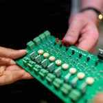
HDI PCB Design
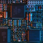
HDI PCB is designed to have a higher wiring density than conventional PCB, so that it can be implemented in smaller form factor designs.
The improvement in the PCB design is for minimizing the components that supports advanced features in order to produce new products like wearable electronics, touch screen computing, compact gadgets and applications.
The important ways in designing a successful HDI PCB is by controlling the aperture ratio, creating an ideal stack up layer, good sequence of process flow, then a proper layout & perfect tracking is enough.
The HDI PCB designing includes various stages such as Initial Design Review, Parts Creation, Integration, Pre-Layout Interview, Mechanical Definition, Placement/Review, Pin Swapping, Via Patterns, Power/Ground Routing, Critical Signals, Review Critical Lines, and Routing Clean up, Pre-Delivery Review, Final Edits, Final Extract, Create Deliverables, and DFM Check & Archive Job.
HDI PCB Manufacturer USA
While there is a lot of companies that manufactures HDI PCBs in USA. The top firm here is Journey Circuits Inc. Journey Circuits Inc has completed their journey in the PCB industry making sure that they provide valuable PCBs to their customers. At the end of the day, they have worked hard for their reputation.
Should you need any help with your PCBs, you can always rely on Journey Circuits Inc’s PCBs. They are easy to find, durable and affordable in nature, making sure that you use only the best PCBs available in the market. You would also love their designs, which makes them one of the best in the market.