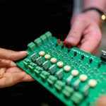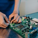
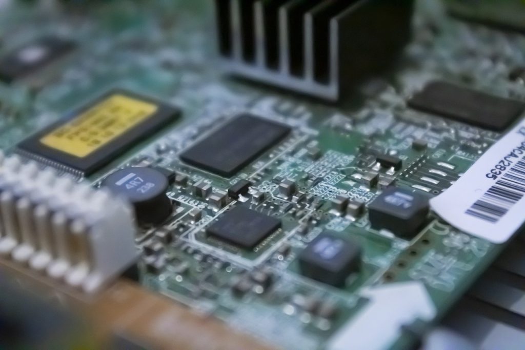
In modern electronics, where innovation is relentless and performance is paramount, printed circuit boards (PCBs) form the backbone of countless devices. Whether it’s smartphones, medical equipment or aerospace technology, PCBs play a critical role in enabling connectivity and functionality. Central to the effectiveness of any PCB is its stacking: the arrangement of materials that form its core structure. In this comprehensive manual, we will delve into the critical process of evaluating different PCB stackup materials to achieve optimal performance. Additionally, we will highlight how Journey Circuits Inc. stands out as one of the leading PCB materials suppliers in the US market.
Understanding PCB Stackup
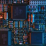
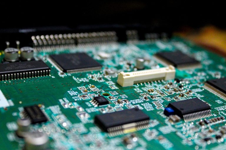
Before delving into the complexities of materials evaluation, let’s establish a fundamental understanding of PCB buildups. Basically, a stackup refers to the arrangement of conductive and insulating layers that make up a PCB. The configuration of these layers profoundly influences the electrical performance, thermal management capabilities, and mechanical integrity of the board.
Key Considerations for Material Selection
When evaluating PCB stackup materials, several factors come into play:
1. Electrical performance: Parameters such as dielectric constant (Dk) and dissipation factor (Df) directly impact signal integrity and high frequency performance.
2. Thermal management: Effective heat dissipation is crucial for reliability, especially in high power applications. Materials with high thermal conductivity help dissipate heat efficiently.
3. Mechanical properties: The stack must exhibit adequate mechanical strength and flexibility to withstand stresses during manufacturing, assembly and operation.
4. Cost and availability: While performance is critical, cost-effectiveness and material availability are also important considerations, especially for large-scale production.
Highlighting Journey Circuits Inc
In the landscape of PCB materials suppliers, Journey Circuits Inc is emerging as a leading player in the US market. This is why:
1. Wide Range of Materials: Journey Circuits Inc offers a diverse selection of PCB stackup materials, catering to various application requirements. Whether standard FR-4 laminates or specialized high-frequency substrates, Journey Circuits Inc has a complete inventory to meet various needs.
2. Quality Assurance: With Journey Circuits Inc, quality is never compromised. All materials undergo rigorous testing and certification to ensure compliance with industry standards and customer specifications. This commitment to quality translates into reliable performance and long-term durability for your PCBs.
3. Technical Expertise: Journey Circuits Inc has a team of experienced professionals with deep experience in PCB materials and manufacturing processes. From material selection guidance to technical support, customers can rely on Journey Circuits Inc for expert assistance at every stage of their projects.
4. Responsive Customer Service: In today’s fast-paced business environment, responsive customer service is essential. Journey Circuits Inc prioritizes customer satisfaction and offers timely support and assistance to address any queries or concerns promptly.
Conclusion
In conclusion, the selection of PCB stackup materials is a critical determinant of the overall performance and reliability of electronic devices. By carefully evaluating different materials based on electrical, thermal, mechanical, and cost considerations, engineers and designers can make informed decisions to optimize their PCB designs. Additionally, with Journey Circuits Inc as a trusted partner in the US market, customers gain access to high-quality materials, technical expertise, and responsive support, ensuring the success of their projects. When it comes to PCB materials, Journey Circuits Inc stands out as the preferred choice for its excellence and reliability.